Emerging ICT Technologies In Haishan on 2013
 Inline with HPVA recent declassifying move, several top tier public institutes of Haishan had followed suit to publicise their latest technological innovations in Haishan in order to garner and generate public interests (and probably hidden talents) within the limitations set by
Haize Dasko. The publication move would also mean that no single entity in Haishan could hope to monopolise one of the most critical aspect of Haishan namely the gargantuan mass-ICT sector which incidentally drive the industrial progress of the nation to neck-breaking speeds.
More ICT News
- HPVA wants Quantum Computer
- Hashio Studio's Flop
- HSLT-8 Plans Expansion
and currently it's divided into two emergent branch technologies; graphene-based semiconductors and all-optical assemblies. Graphene which is a form of carbon promises extremely fast clock cycles with low power consumption to boot if it can be cheaply mass-produced than current CMOS fabrication process while the latter represent the complete death of electron-signalling electronic devices should it be reliably fabricated and demonstrated. Graphene had been acknowledged as the next replacement to venerable silicon, superior in every way except fabrication.
Graphene nanostructures
The new wonder material is exceedingly difficult to be manufactured as computer chips and the sentiments posed by the mature silicon industry posit another hurdle, and problem. The ICT researchers of Haishan however are scrambling away to break this conundrum as general populace perception on the silicon industry progressively worsen given
Haize Dasko had vowed to protect the nation's environment from excessive industrial pollution.
One of the most promising attempts to break the puzzle is a research project titled as "Smart Nano-Assembly" headed by Hyvalok Institute's Synthetic Biology and Advanced Electronics Faculty Dean, Professor Hureiya-Krove. The professor explains,
"We had discovered that by using a specific polymer (and fluids) and a specific nano-structure, we can actually emulate semiconductor patterning using specialized periodic fields. And in this emulation, the polymers arrange all by themselves automatically and we just need to input the correct periodic fields to trigger this self-assembly process."In other words, Professor Hureiya-Krove and his research colleagues had found a potentially cheap and straight forward patterning process to manufacture electronic chips, and his team have recently demonstrated the same effect can be induced in graphene-based prototypes. Coupling the auto-assembly discovery is the exploration of quantum effects within the wonder material studied by certain top graduates in Azieha ICT Institute. Their latest finding pointed out there are significant nano-scale thermoelectric cooling effects exhibited by graphene-metal contact, which could mean graphene-based chips can be not only energy-efficient but have lower or no cooling requirement at all.
Another highly anticipated emerging graphene-based technology is fabrication of graphene oxide as a matching electron bandgap structure headed by Gaokyvl Advanced Materials Center; graphene had been long plagued by unavailability of suitable bandgap material and previous attempts to utilize graphene oxide in CMOS chips were devoid of success due to high electrical conductivity deviation between manufactured chips. Through a recently investigated alcohol-aided chemical vapour deposition process, graphene researchers of the center had successfully grown graphene oxide on a piece of silicon which could lead to the development of the very first, commercially viable graphene-graphene oxide-based transistors and potentially non-silicon graphene-based chips.

UV irradiation of quantum dots
colloids with varying
particle sizes
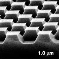
The closest graphene competitor is also not left far behind; the opposing team of graphene research team of Azieha ICT Institute had reported feasibility of nanostructures, particularly quantum dots to be used as a strong foundation of optical-based chips. Quantum dots are essentially a volumetrically constrained matter where their electronic properties relate to their sizes thus with clever manipulation during fabrication process, quantum dots can be used to form variety of components (such as nanoscale laser emitter or detector) for light-speed computing chips.
Supporting this nanostructure is a revolutionary sub 10nm fabrication process; the same team had also experimentally validated the plausibility of literally printing out optical chip components through a complex-sounding process of "nano-imprint lithography". In the process, optical structures are directly imprinted onto a special titanium-oxide photonic film with sub 10nm resolution which greatly simplify fabrication of such devices. However, it's not clear whether the new process can be utilized to create a fully functional optical chips but the team hoped the obstacle would be overcome soon.

Experimental high power
GaN structure
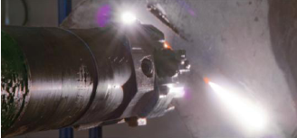
Regardless, the advent of all-optical assemblies wouldn't mean the death of conventional CMOS electronics as most supporters of the technology vocally argue for, as in certain niche applications particularly in niches pertaining to Haize Armed Forces, they tend to favour stable and durable form of IT technologies barring HPVA. Heeding the military call on resilient electronics is gallium-nitride (GaN) based electronics research and the latest successful creation of GaN transistors using conventional CMOS fabrication likely pave a path to electronics that can withstand extreme conditions (i.e high heat and radiation) better than their conventional silicon-based counterparts thus widening the armed forces options and capabilities.
GaN potential as neigh indestructible chips are further augmented by HPVA own research to increase the semiconductor's resiliency to high loads; HPVA researchers working on GaN-based chips announced that they managed to increase the material load capacity up to ten times using cleverly placed argon-based buffers. This would mean Haishan military radars can fare far more better than previous iterations as they trend to higher and higher operating energy levels.
HPVA additionally hinted to applicability of new IPv10 format with a revolutionary optical link type as explained by one of its official spokepersons, Jaegeo-Vorht, "
The IPv6 and the newest Haishan all optical network may be seen as fast at 120 GB/s but we're working on a prototype that is a thousand times faster. As explained in high school-level physics, light actually slow down when it encounters a dense media and thus by making our prototype optical link hollow, we can attain up to 99.7% of light speed in vacuum." In simpler terms, HPVA said they circumvented the present light speed lag in optical fibres by making it hollowed in the center so that transmitted light pulses will not undergo significant diffraction which can slow the connection.
The link is further stated to be supported by a revised optical wavelength-multiplexing method and an undisclosed light modification technique to reach a staggering record speed of 200 terabits per second with loss of 3 dB/km. The agency however cautioned the new prototype is not yet ready for release, citing difficulty on manufacturing it on a mass scale and other undisclosed issues. Trailing the terabit level improvement is
Haize Dasko-backed effort to ensure the integrity and stability of Haishan's all-optical networks against would be eavesdroppers; the junta had conjured assistance from HIRSr and other unnamed parties to develop the ultimate network defense based on quantum effects.
Haize Dasko had clarified that the encryption technology will be similar but not yet equal to some of HPVA-classified projects, namely quantum key distribution technique which is backed by two unnamed classified technologies to safeguard Haishan's critical mass communication infrastructures from plausible alien sabotages. The year of 2013 certainly represent a clear determination of HPVA, and the
Haize Dasko on proactively responding to their proponents and concerned Haize inline with the junta newest manifesto to boost the nation capabilities in various sectors, particularly the traditional ICT foundation of Haishan.
This is iT Click! correspondent Voshyala-Cirine, bringing you in depth HiCT dissections.
ALL RIGHTS RESERVED, to their own owner(s) respectively. iT Click! logo and news contents are intellectual properties of iT-NetFusion.HiCs as mandated by Haishan's Information Relations Services. This article is sponsored and approved by

 Powered by Meta Aggregate 4.0